In this post I describe steps to create a STM32 project for creating complementary PWM outputs with dead time in between. I use STM32CubeMx tool to configure and create a project that is almost ready to compile. I use STM32F4Discovery development kit which has STM32F407 MCU on it. This MCU contains many Timers with different capabilities. You can check out my blog post about STM32 timers for a table of features. We will use TIM1 which have the complementary output feature that we are looking for.
What is “dead time”
First of all, this is what we are trying to achive:
In this diagram we have 2 complementary signals. When one is ON, the other is OFF. They should never be open at the same time. Bu what is dead time, why is it required? Well, electronics aren’t perfect. However fast they are MOSFETs take some time to turn on and off. If two complementary MOSFETs are triggered at the same time, opening one and closing other, during the transition time there is a strong chance that both will be open at the same time. This may be catastrophic and cause immediate failure of the components. To ensure safe operation we put some duration between closing of one and opening other component. This time is usually called dead time in PWM context.
Creating a STM32F4 project using STM32CubeMx
Start STM32CubeMx
STM32CubeMx is a project configuration and generation tool released by ST to ease the life of developers. It creates project using STs HAL libraries. It can generate projects for various IDEs and even pure Makefiles.
Selecting MCU
Click “New Project” in the launch page.
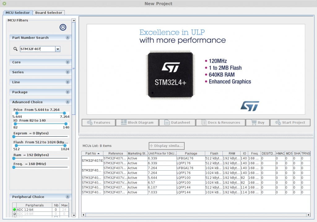
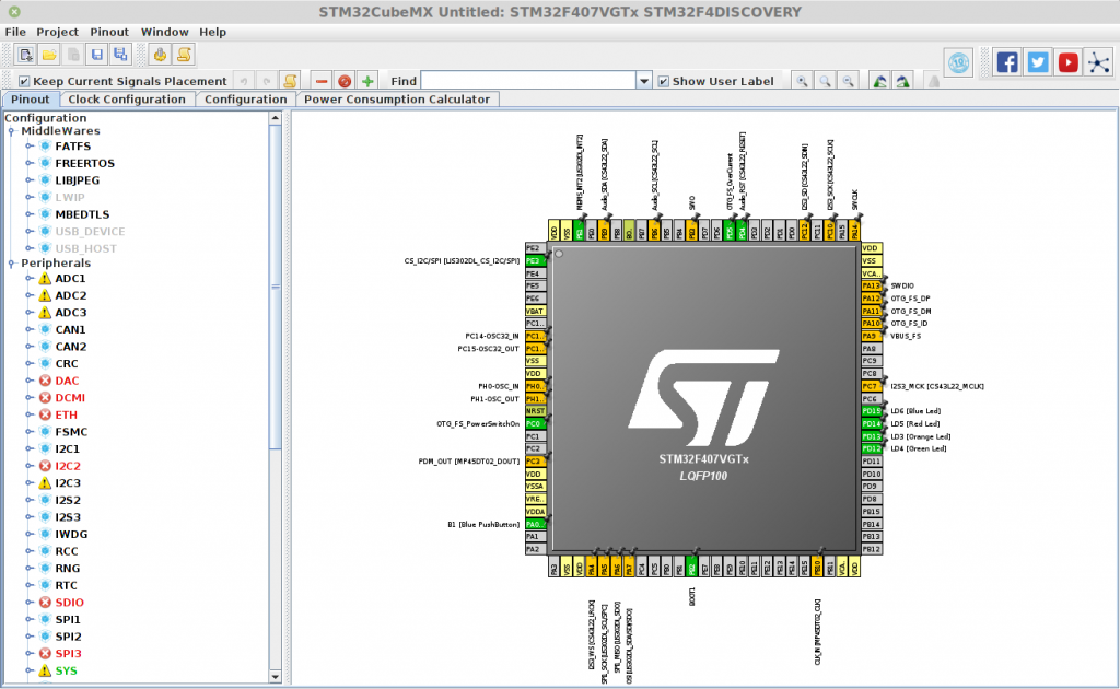
Find and select STM32F407VG MCU from the list. Or you can switch to “Board Selector” tab and select “STM32F4Discovery” kit. In latter case, Cube does some more configuration such as naming pins and configuring them for respective components on the board. But this is not necessary for our use case at the moment.
In case you selected Discovery kit you should see this appear:
Configuring Pins
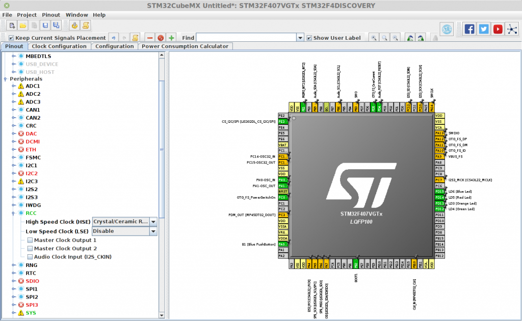
To enable the external 8 MHz crystal, from the component tree, RCC Component module, for “High Speed Clock” option select “Crystal/Ceramic Osc.” option.
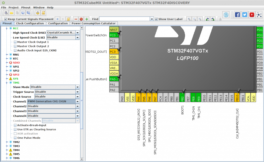
From TIM1 component, change the “Channel1” option to “PWM Generation CH1 CH1N”. When you do that, pins PE8 and PE9 should change state on the pin display. But for you some other pins may be selected since there are alternative pins for TIM1 outputs (as its the case for many other functions of this chip). Just note which pins are selected. Or you can force it to select these pins by manual selection. A tip, when you Alt+LeftClick on a pin, alternatives for it are highlighted.
Configuring Clocks
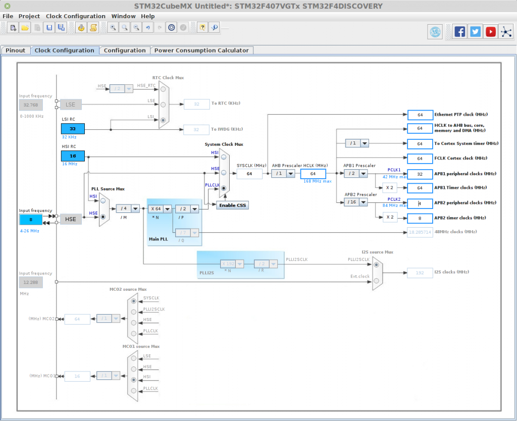
Switch to the “Clock Configuration” tab. For this example, we will set our timer clock to 8MHz. STM32CubeMx has a smart solver. When you type a number to any of the editable boxes it tries to find appropriate configuration values to achieve that clock value. If it fails, it will tell you that value isn’t valid. First, from the “PLL source Mux” section, select the “HSE” option. This will connect our external crystal to PLL input. Don’t mind the errors yet.
TIM1 input clock is supplied from APB2 bus. But as you may have noticed timers clock input is twice the bus clock and they have dedicated box to set frequency. Click on the “APB2 Timer Clocks” box and enter “8”. Click any other box so that Cube updates the configuration. It should analyze and find a suitable configuration almost immediately. You can try to change system clock etc. yourself. For reference you should have something like this at the end:
Configuring Timer module
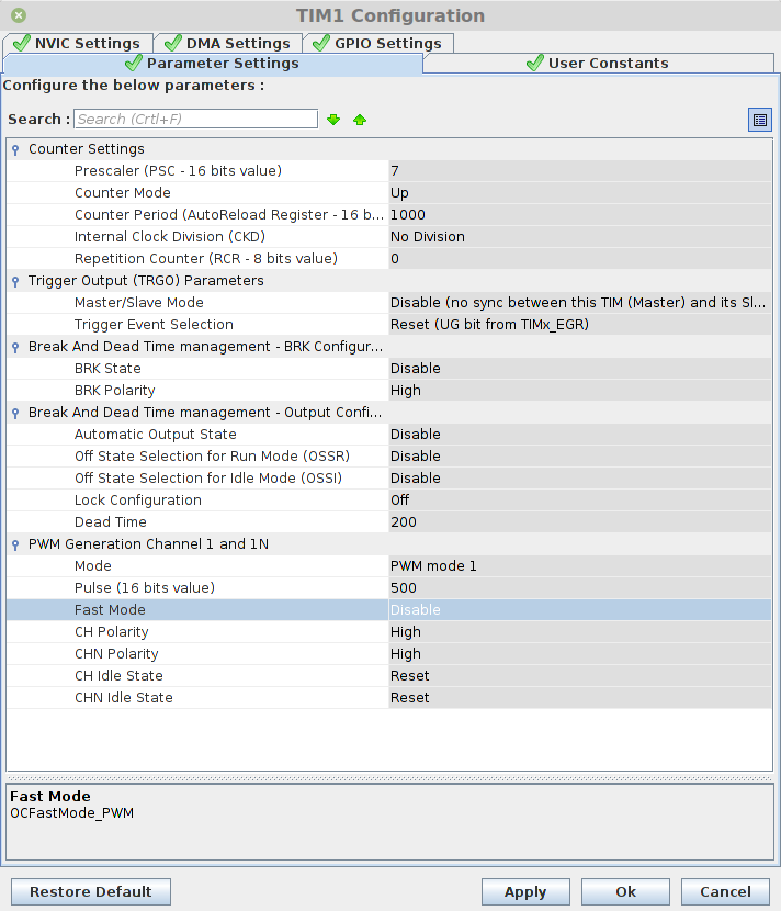
Switch to the “Configuration” tab. From the “Control” box, click the “TIM1” button. Below window should appear.
If you want to understand what all these options mean it’s a good idea to read reference manual. At the moment I will stick to the bare minimum.
First option you should set is the “Prescaler”. This slows down the timer input clock so that longer durations are possible. Also it makes it easier to achieve a particular duration value since you can enter any number between 0-65535. This value “+ 1” will be used the divide the input clock. Our timer input clock is 8MHz, to divide it to 8 and obtain 1MHz timer clock we should set prescaler to 7.
To set PWM signal period, change the “Counter Period” option. Set it to 1000, to have a 1ms waveform.
To enable dead time insertion enter “200” in to the “Dead Time” option. Note that, this won’t doesn’t result in a 200µs dead time duration. Dead time setting and the actual duration of dead time will be explained later.
To set PWM signal duty cycle, set the “Pulse” option for the Channel 1. To have a 50% duty cycle enter 500. In the end you should have a configuration like this:
Generating the Project
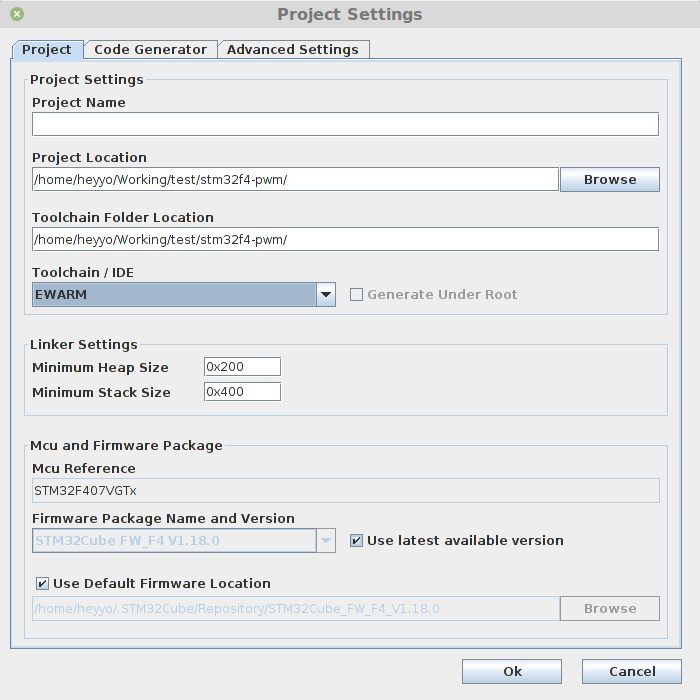
From the Project menu, select the “Generate Project”. Enter project name and location. Select the toolchain/IDE you want to use. Note that STM32CubeMx itself doesn’t provide any IDE or compiler. You have to setup the IDE yourself. When clicked “OK”, Cube may ask about some downloads. Select Ok, and wait until they complete. At the end, project should be created in selected location.
Code additions
Before compiling the project some additions should be made to actually enable the PWM outputs. Open the “main.c” file add these lines before the main “while” loop.
/* USER CODE BEGIN 2 */
HAL_TIM_PWM_Start(&htim1, TIM_CHANNEL_1);
HAL_TIMEx_PWMN_Start(&htim1, TIM_CHANNEL_1); // turn on complementary channel
/* USER CODE END 2 */
Be careful to add code in between “user code” comments. When you change the configuration and re-generate the project, Cube will make sure these lines are retained. Any other line that is not inside “user code” comments will be deleted.
That should be all. Compile and flash.
Duration of the Dead Time
Dead time setting is an 8 bit value. As a result it can be set between 0-255. This setting configures dead time duration in respect to the timer input clock. Note that this clock is before the “prescaler”. In our example, timer running frequency is 1 MHz but input frequency is 8 MHz. Dead time is determined from this clock. That means dead time duration is set in ( 1 / 8MHz = 125ns) steps. But that’s not all! I believe, to make it possible to set even greater durations, ST made things a little complicated. Here are the rules:
X as the the dead time setting, T actual dead time duration, t clock period (125ns in our case);
If X <= 127:

    T = X * t ⇛ in between 0 .. 127t

If X >= 128 and X <= 191:

    T = (64 + (X[5..0])) * 2 * t ⇛ in between 128t .. 254t

If X >= 192 and X <= 223:

    T = (32 + (X[4..0])) * 8 * t ⇛ in between 256t .. 504t

If X >= 224:

    T = (32 + (X[4..0])) * 16 * t ⇛ in between 512t .. 1008t
Let’s see how we can calculate the required setting for a desired duration with an example. For example, lets say we want 75µs dead time duration and our timer clock is 8MHz which means 125ns steps (t). Dividing 75µs to 125ns we need 600t setting. This means the X should be in the region of X >= 224 (4th option). Extract the offset portion of the 600t duration, which is 32 * 16 * t = 512t. Result is 600t - 512t = 88t. Divide this to multiplier, 16. Resulting: 88t / 16 = 5,5t. As you can see, we arrived at a fractional number, which means we cannot obtain an exact 75µs duration. We have to settle for a little bit less or more. Lets pick 6. Add this to the “224” to have the final setting value of, X = 224 + 6 = 230. This should give us 76µs dead time duration.
I hope this explanation was clear. If you didn’t understand, please read the description of TIMx_BDTR register in the manual (DTG bits).


19 responses to “STM32 PWM Output with Dead Time Using STM32Cube HAL Platform”
Thank you very much for this post! Helpful and clear!
STM32CubeMX can be really complicated to configure … And it takes a long time to find and understand all the parameters …
Even for simple things (like PWM dead times :p ).
Merhaba bitirme projesi olarak stm32 ile Fırçasız Dc motor sürücü tasarımı yapıyorum yaptığım hatalar bana pahalıya patlıyor örnek alabileceğim uygulamalar konusunda yardımcı olabilirseniz sevinirim. Teşekkür ederim başarılar dilerim.
Maalesef güç elektroniği konusunda pek bilgim yok. Bu çalışmayı da hocam için yapmıştım. Arkadaşım çok uğraştı, çok mosfet yaktı 😀 Ben masanın arkasına saklanarak seyrettim dumanları! Zor bir işe kalkışmışsın. İstersen arkadaşımı sana yönlendirebilirim, onun biraz faydası olabilir sana bu konuda.
Merhaba. half-bridge DC-DC converter tasarliyorum. Mosfetlerimi stm32 mikroislemcisi ile kontrol edecegim. Islemciden ayni duty’li 2 PWM sinyali elde etmem gerekiyor. Bunu stm32f334c8Tx islemcisinde HRTIM ile yapabilecegimi ögrendim. Ama HRTIM ile basic bir single PWM bile üretemedim. TIM1 üzerinden yapabiliyorum fakat HRTIM konusunda yardima ihtiyacim var. Bahsettiginiz arkadasiniz ile iletisime gecmem mümkün müdür? Muhtemelen arayüzden gerekli ayarlamalari da yaptim fakat kod kisminda Start edicek kodu yazamadim. Bu genc mühendis adayina bir el uzatin lütfen:)
Hâlâ ihtiyacınız varsa yardımcı olabilirim
Where did these formula come from. I cannot find any reference to them anywhere else?
Graham, It has been some time, I haven’t worked on this recently.
If you are asking about the formulas related to “duration of the dead time”, I believe I have derived those from the definitions of “DTG” field of “TIMx_BDTR” register. You can find it in the STM32F4 reference manual (RM0090). Search for “Dead-time generator setup”.
Hi
Could you please help me with phase shift in PWM using CUBEMX.
Thanks
I’m sorry I didn’t work on this for a long time. I can’t.
Very helpful thank you !!!
Awesome explanation but my “complimentary PWM” TIMx-CH1 is exactly the inverse of TIMx-CH1N. Not like having one waveform offset from the other as per your image at the beginning.
Selamlar iyi çalışmalar, ben waijung block setleriyle bir türlü 5 usn ölü zaman alamıyorum. Yardımcı olabilir misiniz
Bahsettiğiniz yazılımı hiç bilmiyorum. Burda limitleyici faktör timer’ın giriş frekansı. Eğer kullandığınız yazılım size timer frekansı ve/veya dead time register’larına direkt erişim vermiyorsa, ne yapılabilir bilemiyorum.
I am using stm32f401VE controller to drive IM using spwm and open loop V/F method. I configured carrier frequency as 4KHZ and creating sine signal in TIM2 which is of 100usec.computation of compare count for the sine wave is happening in TIM1 update event which should be theoretically 250usec.
I configured TIM1 as clock 84MHz,prescale value is 7, PWM mode 2, centre aligned mode. I calculated value for 2625 for getting period 250usec(4khz) or half 125usec for centre aligned method(1312). Interrupt priority is set as TIM1 is 0 and TIM2 is 1.
Execution time of ISR TIM1 is 12usec and TIM2 is 36usec
Following are my observations
1. Update event is happening in 124usec which supposed to be at 125usec
2. If i compute compare count value in TIM2 sometimes i missed update event. The pwm switching frequency period is varying e.g. for 4khz it should be 250us but sometimes its 244us, sometimes 248 etc. and found that even the interrupt time varies and hence the pwm frequency is not constant.
Pls suggest
Hi, Nice article.
I have few issues i am facing with my control board with STM32F401VE.
I configured TIM1 as clock 84MHz,prescale value is 7, PWM mode 2, centre aligned mode. I calculated value for 2625 for getting period 250usec or half 125usec for centre aligned method(1312). Interrupt priority is set as TIM1 is 0 and TIM2 is 1.
Execution time of ISR TIM1 is 12usec and TIM2 is 36usec.
But i find that pwm switching frequency as in this case say 250us(4khz) is varying from 244us to 248us its not exact 250us. Also the interrupt times varies and hence the PWM switching time.
Pls suggest
Regards,
Mukesh
Hello sir,
I’m working with BLDC Motor Controller,
For my hardware design, i want dead time to inserted in high side pulse.
Can you please suggest me how to set that in stm32
When duty cycle is set to 100%, there is still a dead-time visible. One would expect a constant high signal, but it goes to low every cycle and stays there for the configured dead-time… Really annoying.
Merhabalar sayın hocam , ben 180 derece zıt fazda iki adet %40 duty li 100kHz lik sinyali stm32 kartı ile üretmeye çalışıyorumda size bir sorum olacaktı stm32f103 kartı ile bunu yapmak mümkünmüdür acaba ve istediğimiz miktarda dead time ayarlayabilirmiyiz , üzerine çalıştığım proje için yardımcı olabilirseniz çok sevinirim , TEŞEKKÜRLER..
For everyone asking where the calculations come from:
reference manual of STM32H723
Bits 7:0 DTG[7:0]: Dead-time generator setup
This bit-field defines the duration of the dead-time inserted between the complementary
outputs. DT correspond to this duration.
DTG[7:5] = 0xx => DT = DTG[7:0] x tdtg with tdtg = tDTS
DTG[7:5] = 10x => DT = (64 + DTG[5:0]) x tdtg with tdtg = 2 x tDTS
DTG[7:5] = 110 => DT = (32 + DTG[4:0]) x tdtg with tdtg = 8 x tDTS
DTG[7:5] = 111 => DT = (32 + DTG[4:0]) x tdtg with tdtg = 16 x tDTS
Example if tDTS = 125 ns (8 MHz), dead-time possible values are:
0 to 15875 ns by 125 ns steps,
16 µs to 31750 ns by 250 ns steps,
32 µs to 63 µs by 1 µs steps,
64 µs to 126 µs by 2 µs steps
Note: This bit-field can not be modified as long as LOCK level 1, 2 or 3 has been programmed
(LOCK bits in TIMx_BDTR register)